30/5/15

Việt Nam chế tạo thành công vi mạch chuyên dụng mã hoá video đầu tiên


Giảng viên trường Đại học Công nghệ, Đại học Quốc gia Hà Nội nghiên cứu và chế tạo thành công vi mạch chuyên dụng mã hoá video đầu tiên tại Việt Nam, có thể ứng dụng trong lĩnh vực quốc phòng, an ninh.

Sáng 18/5/2015, trường ĐH Công nghệ (ĐH Quốc gia Hà Nội) công bố thông tin về sản phẩm vi mạch VNU-UET VENGME H.264/AVC @2014 (gọi tắt là VENGME H.264/AVC). Đây là vi mạch chuyên dụng mã hoá video đầu tiên của Việt Nam.

Đề tài do PGS Trần Xuân Tú chủ trì đã thiết kế, xây dựng kiến trúc phần cứng để thực hiện chức năng mã hoá video tương thích với chuẩn H.264/AVC dùng cho các thiết bị di động. Sau khi thiết kế thành công, bản thiết kế đã được gửi đi sản xuất tại hãng Global Foundry với công nghệ bán dẫn CMOS 130 nm.

VENGME H.264/AVC là vi mạch chuyên dụng thế hệ vi mạch đang được sử dụng rộng rãi nhất trên thế giới hiện nay và có độ phức tạp rất cao, tích hợp trên hai triệu cổng lô-gic (tương đương 8 triệu transistors). Ngoài việc tiếp cận, nắm vững công nghệ thiết kế đáp ứng chức năng mã hóa theo chuẩn của vi mạch, nhóm nghiên cứu còn có một số phát triển giải pháp tối ưu riêng, như kỹ thuật xử lý đường ống 4 tầng, phương pháp tái sử dụng dữ liệu, kỹ thuật tính toán trong quá trình truyền dữ liệu giữa các khối cơ bản, kỹ thuật thiết kế công suất thấp.


Vi mạch mã hóa video VNU-UET VENGME H.264/AVC @2014 do nhóm nghiên cứu của PGS Trần Xuân Tú thiết kế và chế tạo. (Ảnh: Bùi Tuấn).

Vi mạch có một số tính năng vượt trội so với các sản phẩm công nghệ cùng lĩnh vực ứng dụng đang được nghiên cứu và triển khai trên thế giới về hiệu năng, năng lượng tiêu thụ và giá thành thiết kế. Nó có thể xử lý thời gian thực các video có độ phân giải lên tới HD 720p ở tần số 100MHz, với công suất tiêu thụ khá nhỏ (53 mW). Các nội dung sáng tạo này là cơ sở để nhóm tác giả công bố 10 bài báo trong hệ thống ISI/Scopus và được cộng đồng khoa học quốc tế quan tâm, trích dẫn đến 26 lần.

Qua nghiên cứu, trường Đại học Công nghệ đã xây dựng một đội ngũ cán bộ khoa học tương đối mạnh, làm chủ công nghệ thiết kế mạch tích hợp và có khả năng giải quyết các vấn đề công nghệ hiện đại, cho phép triển khai thiết kế các vi mạch quan trọng phục vụ cho lĩnh vực quốc phòng và an ninh quốc gia bằng nội lực.

Vi mạch mã hoá tín hiệu video VENGME H.264/AVC được thiết kế nhằm hướng tới các ứng dụng như camera an ninh, camera giao thông, camera giám sát hiện trường hay đơn giản là camera giám sát toà nhà, trường học, địa điểm công cộng… và các thiết bị di động như điện thoại thông minh, máy quay video. Tại lễ công bố, trường Đại học Công nghệ và Công ty TNHH Giải pháp Thông minh Sài Gòn đã ký thoả thuận chuyển giao công nghệ và hợp tác phát triển thiết bị ứng dụng đối với VENGME H.264/AVC.

Sản phẩm công nghệ của đề tài cũng đã được chia sẻ một phần với Viện Điện tử và Tin học thuộc Uỷ ban năng lượng nguyên tử (CEA-LETI) của Cộng hoà Pháp để tiếp tục phát triển theo hướng giảm sâu công suất tiêu thụ - một trong những yêu cầu ngày càng gắt gao của các thiết bị di động hướng công nghệ xanh.

Ông Nguyễn Thanh Bình, Vụ trưởng Vụ Khoa học Công nghệ (Ban Cơ yếu Chính phủ) cho biết Ban Cơ yếu cũng đặt mục tiêu sớm thiết kế một vi mạch để sử dụng trong ngành. "Chúng tôi có những buổi làm việc với PGS Tú và thấy khả năng hợp tác sau buổi công bố rất khả quan. Dù chặng đường đi đến sản phẩm còn dài, nhưng đây là bước khởi đầu của định hướng phát triển công nghệ, công nghệ chất lượng cao dần dần thay thế lao động gia công", ông Bình nói.

"Chương trình phát triển sản phẩm quốc gia định hướng phát triển vi mạch, Quỹ đổi mới công nghệ cũng đặt mục tiêu phát triển vi mạch điện tử là 1 trong những hướng chủ đạo. Bộ Khoa học công nghệ vì thế sẽ tạo điều kiện để các đơn vị nghiên cứu và đào tạo có thể tham gia đồng hành vào các chương trình của Bộ Khoa học công nghệ", ông Nguyễn Văn Tăng, đại diện Văn phòng chương trình phát triển sản phẩm quốc gia (Bộ Khoa học Công nghệ), khẳng định.

Vi mạch là phần cơ bản, mấu chốt trong tất cả các sản phẩm công nghiệp, nhất là công nghiệp điện tử, và có thể được ví như "gạo công nghiệp". Việc chủ động sản xuất được các dòng vi mạch điện tử có chức năng đa dạng và cập nhật công nghệ hiện đại nhất của thế giới sẽ nâng cao giá trị sản phẩm điện tử sản xuất tại Việt Nam với mức lợi nhuận đến 30%. Nghiên cứu và chế tạo thành công vi mạch còn đóng góp vào công tác đào tạo nguồn nhân lực chất lượng cao cho nền kinh tế tri thức, giảm nhập siêu linh kiện điện tử và giải pháp công nghệ, tạo ra các sản phẩm có ảnh hưởng và tác động lớn đến sự phát triển của nền kinh tế đất nước.

Với sản phẩm này, Việt Nam còn có thể làm chủ công nghệ điện tử phục vụ an ninh quốc phòng, thiết kế và chế tạo vi mạch điện tử quan trọng trong hệ thống vũ khí, khí tài quân sự, hệ thống định vị mục tiêu; bảo mật thông tin. Đây là những vấn đề không thể đặt hàng hoặc thuê nước ngoài thiết kế và chế tạo.

Ông Nguyễn Hữu Đức, phó Giám đốc ĐH Quốc gia Hà Nội, đánh giá nhóm nghiên cứu của PGS Trần Xuân Tú đã kết hợp tốt các quan điểm về nghiên cứu gắn thực tiễn và hội nhập quốc tế (xuất phát từ yêu cầu thực tiễn của đất nước, nhưng cần được triển khai theo cách tiếp cận chuẩn mực quốc tế); nghiên cứu cơ bản và phát triển công nghệ với trình độ cao (đảm bảo phát hiện tri thức mới, giải pháp mới có giá trị công bố được được trên các tạp chí quốc tế, hoặc đăng ký phát minh, sáng chế) và quan điểm nghiên cứu ứng dụng có hàm lượng khoa học cao.

"Cùng với chương trình phát triển công nghiệp vi mạch Thành phố Hồ Chí Minh, sản phẩm vi mạch mã hoá video VENGME H.264/AVC của Đại học Quốc gia Hà Nội góp phần nâng cao vị thế của Việt Nam trên bản đồ sản xuất chip của thế giới, củng cố vị trí thứ 3 trong khu vực ASEAN. Đại học Quốc gia Hà Nội sẽ tiếp tục hỗ trợ, đầu tư để nhóm nghiên cứu phát triển ứng dụng của vi mạch đã chế tạo được và phát triển các thế hệ vi mạch mới có thể cạnh tranh toàn cầu", GS Nguyễn Hữu Đức nói.

Nguồn khoahoc.tv

25/5/15

ZedBoard Zynq™-7000 Development Board - DIGILENT


Part: 410-248P-KIT
  • Đơn giá:  Liên hệ
  • Xuất sứ: Taiwan.
  • Tên sản phẩm: ZedBoard  Zynq™-7000 Development Board
  • Tấm mạch in đã lắp ráp hoàn chỉnh và phụ kiện đi kèm dùng cho nghiên cứu phát triển vi mạch. Bộ chuyển đổi cho vi xử lý. 
  • Nhà sản xuất: Digilent. Hàng mới 100%.
  • Liên hệ: 0935 408 286 or 0934 993 253
IC: 
  • Xilinx Zynq™-7000 All Programmable SoC (AP SoC) (XC7Z020-CLG484)
  • Analog Devices ADV7511 High Performance 225 MHz HDMI® Transmitter
  • Analog Devices ADAU1761 SigmaDSP® Stereo, Low Power, 96 kHz, 24-Bit Audio Codec
Programming:
  • Onboard USB-JTAG Programming
Features:
  • Zynq-7000 AP SoC XC7Z020-CLG484
  • Dual-core ARM Cortex A9
  • Memory:
  • 512 MB DDR3
  • 256 Mb Quad-SPI Flash
  • 4 GB SD card
  • Onboard USB-JTAG Programming
  • 10/100/1000 Ethernet
  • USB OTG 2.0 and USB-UART
  • PS & PL I/O expansion (FMC, Pmod™, XADC)
  • Multiple displays (1080p HDMI, 8-bit VGA, 128 x 32 OLED)
  • I2S Audio CODEC
Target Applications:
  • Video processing
  • Motor control
  • Software acceleration
  • Linux/Android/RTOS development
  • Embedded ARM® processing
  • General Zynq™-7000 AP SoC prototyping
Linh Kiện Mạch - Mạch Thí Nghiệm FPGAZedBoard is a low-cost development board for the Xilinx Zynq™-7000 All Programmable SoC (AP SoC). This board contains everything necessary to create a Linux, Android, Windows® or other OS/RTOS based design. Additionally, several expansion connectors expose the processing system and programmable logic I/Os for easy user access. 

Take advantage of the Zynq-7000 AP SoC’s tightly coupled ARM® processing system and 7 series programmable logic to create unique and powerful designs with the ZedBoard. The ZedBoard kit is supported by the www.zedboard.org community website where users can collaborate with other engineers also working on Zynq designs.

Kit Includes:
  • Avnet ZedBoard 7020 baseboard
  • 12 V AC/DC power supply
  • 4 GB SD Card
  • Micro-USB cable
  • USB Adapter: Male Micro-B to Female Standard-A
  • Getting Started Guide
  • Vivado® Design Suite with device-locked Design Edition license
Cung cấp Linh Kiện Mạch - Mạch Thí Nghiệm FPGA.

  • If you would like an evaluation board for academic purposes, you can apply for a donation through the Xilinx University Program.
  • For more information or product support, please visit:  http://www.zedboard.org/.
  • Want to master the Xilinx Zynq SoC on your ZedBoard? Take a look at "The ZYNQ Book", an accessible, readable book written for people just starting out with Zynq, as well as engineers already working with Zynq. You can download it free (or purchase a hard copy) at http://www.zynqbook.com/.


HotLine: 0935.408.286 or 0934 993 253
Skype: linhkienmach
 Email: linhkienmach@gmail.com
Fanpage: Linh Kiện Mạch - Mạch Thí Nghiệm FPGA

15/5/15

ZYBO Zynq™-7000 Development Board - DIGILENT


Part: 410-279P-KIT
  • Đơn giá:  Liên hệ
  • Xuất sứ: Taiwan.
  • Tên sản phẩm: ZYBO Zynq™-7000 Development Board
  • Tấm mạch in đã lắp ráp hoàn chỉnh và phụ kiện đi kèm dùng cho nghiên cứu phát triển vi mạch SoC. 
  • Nhà sản xuất: Digilent. Hàng mới 100%.
  • Liên hệ: 0935 408 286 or 0934 993 253

IC: Xilinx Zynq-7000 (Z-7010)

The Z-7010 features include:
  • 650Mhz dual-core Cortex-A9 processor
  • DDR3 memory controller with 8 DMA channels
  • High-bandwith peripheral controllers: 1G Ethernet, USB 2.0, SDIO
  • Low-bandwidth peripheral controller: SPI, UART, I2C
  • Reprogrammable logic equivalent to Artix-7 FPGA
- 28K logic cells
- 240KB Block RAM
- 80 DSP slices
- On-chip dual channel, 12-bit, 1 MSPS analog-to-digital converter (XADC)
The ZYBO offers the following on-board ports and peripherals:
  • ZYNQ XC7Z010-1CLG400C
  • 512MB x32 DDR3 w/ 1050Mbps bandwidth
  • Dual-role (Source/Sink) HDMI port
  • 16-bits per pixel VGA output port
  • Trimode (1Gbit/100Mbit/10Mbit) Ethernet PHY
  • MicroSD slot (supports Linux file system)
  • OTG USB 2.0 PHY (supports host and device)
  • External EEPROM (programmed with 48-bit globally unique EUI-48/64™ compatible identifier)
  • Audio codec with headphone out, microphone and line in jacks
  • 128Mb Serial Flash w/ QSPI interface
  • On-board JTAG programming and UART to USB converter
  • GPIO: 6 pushbuttons, 4 slide switches, 5 LEDs
  • Six Pmod connectors (1 processor-dedicated, 1 dual analog/digital)
The ZYBO (Zynq Board) is a feature-rich, ready-to-use, entry-level embedded software and digital circuit development platform built around the smallest member of the Xilinx Zynq-7000 family, the Z-7010. The Z-7010 is based on the Xilinx All Programmable System-on-Chip (AP SoC) architecture, which tightly integrates a dual-core ARM Cortex-A9 processor with Xilinx 7-series Field Programmable Gate Array (FPGA) logic. When coupled with the rich set of multimedia and connectivity peripherals available on the ZYBO, the Zynq Z-7010 can host a whole system design. The on-board memories, video and audio I/O, dual-role USB, Ethernet and SD slot will have your design up-and-ready with no additional hardware needed. Additionally, six Pmod connectors are available to put any design on an easy growth path.

Linh Kiện Mạch - Mạch Thí Nghiệm FPGAThe ZYBO provides an ultra-low cost alternative to the ZedBoard for designers that don't require the high-density I/O of the FMC connector, but still wish to leverage the massive processing power and extensibility of the Zynq AP SoC architecture.

The ZYBO is compatible with Xilinx’s new high-performance Vivado Design Suite as well as the ISE/EDK toolset. These toolsets meld FPGA logic design with embedded ARM software development into an easy to use, intuitive design flow. They can be used for designing systems of any complexity, from a complete operating system running multiple server applications in tandem, down to a simple bare-metal program that controls some LEDs. For systems that require an operating system, Digilent provides an out-of-the-box Linux solution specifically targeted to run on the ZYBO, complete with documentation describing how best to mold it to suite your purposes. These Xilinx tools and Linux solution are all available to use at no additional cost with the ZYBO.

Note: The ZYBO ships without accessories. For users needing more, we offer a ZYBO Accessory Kit that contains:
  • Voucher for Xilinx Vivado® Design Suite: Design Edition (One full seat, node locked, device-locked to the Zynq-7000 XC7Z010)
  • 4GB Micro SD card
  • Micro USB cable
  • 5V 2.5A switching power supply
You can bundle an Accessory Kit with your ZYBO at time of purchase for only $20! Additionally, you can purchase a Micro USB cable and 5V power supply from our Accessories category.

Kit Board Mạch Phát Triển


HotLine: 0935.408.286 or 0934 993 253
Skype: linhkienmach
 Email: linhkienmach@gmail.com
Fanpage: Linh Kiện Mạch - Mạch Thí Nghiệm FPGA

28/4/15

GPIO-HSTC Card - Tấm mạch in - Terasic


Interface Conversion
  • [THDB-HTG(F)] GPIO-HSTC Card - Part No: P0024  
  • [THDB-HTG(M)] GPIO-HSTC Card - Part No: P0033  
  • Đơn giá:  Liên hệ
  • Xuất sứ: Taiwan.
  • Tên sản phẩm: GPIO-HSTC Card
  • Tấm mạch in đã được lắp ráp hoàn chỉnh dùng cho giao tiếp với các thiết bị phát triển. 
  • Nhà sản xuất: Terasic. Hàng mới 100%.
  • Liên hệ: 0935 408 286 or 0934 993 253
Overview
Kit Board Mạch Phát Triển

The HTG Card is designed to convert a High-Speed Terasic connector (HSTC) or a High-Speed Mezzanine connector (HSMC) I/Os to three 40-pin expansion prototype connectors, which are compatible with Altera DE3/DE2-115/DE2/DE1/DE0 expansion headers. Users can connect up to three Altera DE3/DE2-115/DE2/DE1/DE0 boards (or associated daughter cards) onto a HSTC/HSMC-interfaced host board via a HTG Card.

Specification
  • Convert HSTC/HSMC-interfaced I/O to standard 40-pin expansion connectors.
  • Allow users to connect Altera DE3/DE2-115/DE2/DE1/DE0 boards to a HSTC/HSMC-interfaced host board.
  • Provide test points for signal measurement
Block diagram


HTG
  • Connect HTG with Altera Cyclone III Starter Board

  • Connect HTG with Altera DE3
Note. An adapter (SFF or HFF) is required to connect ADA-HSMC with DE3. It is bundled in DE3 kit.

  • Connect HTG with Altera DE4
Note. One adapters (HFM2) required to connect DVI-HSMC with DE4. They are bundled in DE4 kit.

  • Connect HTG with Altera DE2-115
Resources

Documents
TitleVersionSize(KB)Date AddedDownload
THDB-HTG User Manua1.0.311502011-07-20

Kit Contents
  • One HTG Card


HotLine: 0935.408.286 or 0934 993 253
Skype: linhkienmach
 Email: linhkienmach@gmail.com
Fanpage: Linh Kiện Mạch - Mạch Thí Nghiệm FPGA

23/4/15

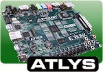
Atlys™ Spartan-6 FPGA Development Board


Linh Kiện Mạch - Mạch Thí Nghiệm FPGA
Part: 410-178P-KIT
  • Đơn giá:   7.900.000 VND
  • Xuất sứ: Taiwan.
  • Tên sản phẩm: Atlys™ Spartan-6 FPGA Development Board
  • Tấm mạch in đã được lắp ráp hoàn chỉnh dùng cho thiết bị phát triển hệ thống nhúng trên FPGA. 
  • Nhà sản xuất: Digilent. Hàng mới 100%.
  • Liên hệ: 0935 408 286 or 0934 993 253

IC: Xilinx Spartan®-6 LX45 FPGA in a 324-pin BGA package
Connector(s):
One Vmod™ (high-speed VHDC) connector
One 12-pin Pmod™ connector
One RJ-45 connector for 10/100/1000 Ethernet PHY and RS-232 serial
Two HDMI video input ports & two HDMI output ports
Two on-board USB2 ports for programming & data transfer
AC-97 audio with line-in, line-out, mic, & headphone
Programming:
JTAG programming interfaces compatible with Xilinx's iMPACT™ and Digilent Adept™
  • Xilinx Spartan-6 LX45 FPGA, 324-pin BGA package
  • 128Mbyte DDR2 16-bit wide data
  • 10/100/1000 Ethernet PHY
  • On-board USB2 ports for programming & data transfer
  • USB-UART and USB-HID port (for mouse/keyboard)
  • Two HDMI video input ports & two HDMI output ports
  • AC-97 Codec with line-in, line-out, mic, & headphone
  • Real time power monitors on all power rails
  • 16Mbyte x4 SPI Flash for configuration & data storage
  • 100MHz CMOS oscillator
  • 48 I/O’s routed to expansion connectors
  • GPIO includes 8 LEDs, 6 buttons, & 8 slide switches
  • Ships with a 20W power supply and USB cable

The Atlys circuit board is a complete, ready-to-use digital circuit development platform based on a Xilinx Spartan 6 LX45 FPGA. The on-board collection of high-end peripherals, including Gbit Ethernet, HDMI Video, 128Mbyte DDR2 memory array, audio and USB ports make the Atlys board an ideal host for complete digital systems built around embedded processors like Xilinx’s MicroBlaze. Atlys is fully compatible with all Xilinx CAD tools, including ChipScope, EDK, and the free WebPack, so designs can be completed with no extra costs.

Linh Kiện Mạch - Mạch Thí Nghiệm FPGA
The Spartan-6 LX45 is optimized for high-performance logic and offers:
  • 6,822 slices each containing four 6-input LUTs and eight flip-flops
  • 2.1Mbits of fast block RAM
  • 4 clock tiles (8 DCMs & 4 PLLs)
  • 6 phased-locked loops
  • 58 DSP slices
  • 500MHz+ clock speeds
The Atlys board can be communicated with and programmed by the Digilent Adept software. In addition, the board can be programmed by Xilinx's iMPACT using the Digilent Plugin for Xilinx Tools.

The required USB-UART driver is available for free download from Exar.

Linux developers: The Atlys board is supported by PetaLinux SDK for an out-of-the-box embedded Linux solution.

Linh Kiện Mạch - Mạch Thí Nghiệm FPGA


Digilentinc

1/12/14

Ngành công nghiệp vi mạch Việt Nam với nhiều kỳ vọng mới!


Bộ Công Thương vừa trình Thủ tướng Chính phủ phê duyệt chủ trương đầu tư cơ chế, chính sách ưu đãi đối với dự án nhà máy sản xuất vi mạch (chip điện tử) của Tổng công ty Công nghiệp Sài Gòn.

Ngành công nghiệp vi mạch Việt Nam với nhiều kỳ vọng mới!

Việc tự sản xuất các vi mạch sẽ góp phần nâng cao giá trị sản phẩm điện tử của Việt Nam

CôngThương - Nền móng cho công nghiệp vi mạch

Là dự án sản xuất vi mạch đầu tiên của nước ta, dự án nhà máy sản xuất vi mạch có vị trí trung tâm trong việc hình thành hệ sinh thái ngành công nghiệp sản xuất vi mạch điện tử của khu vực TP. Hồ Chí Minh và rộng hơn là Việt Nam. Bên cạnh đó, sản phẩm quốc gia vi mạch điện tử chỉ có thể phát triển khi nhà máy sản xuất vi mạch của doanh nghiệp (DN) trong nước đi vào hoạt động. Do đó, dự án cũng được kỳ vọng sẽ trở thành trung tâm để thực hiện các dự án KHCN trong nước, làm chủ công nghệ thiết kế, chế tạo sản phẩm vi mạch điện tử cũng như triển khai những kết quả nghiên cứu về vi mạch điện tử vào thực tế trên quy mô công nghiệp.

Riêng về vấn đề nhân lực, dự án đi vào hoạt động sẽ là trung tâm đầu tiên tại Việt Nam có môi trường thực tiễn phục vụ đào tạo, thực tập, nghiên cứu, nâng cao trình độ cho đội ngũ các nhà khoa học, kỹ sư, sinh viên. Trong tương lai, đội ngũ này sẽ góp phần phục vụ các mục tiêu về phát triển nguồn nhân lực chất lượng cao của ngành công nghiệp điện tử nói chung, ngành công nghiệp sản xuất vi mạch nói riêng.

Sản phẩm chiến lược của Dự án bao gồm chip RFID, chip năng lượng (power IC) và chip điện tử thông dụng (vi điều khiển 8, 16, 32 bit...). Đến năm 2020, dự án được kỳ vọng sẽ cung cấp các sản phẩm đòi hỏi mức độ bảo mật thông tin cao như thẻ định danh cá nhân, thẻ ngân hàng, hệ thống quản lý khí tài quân sự... Sau năm 2020, dự án sẽ từng bước đáp ứng nhu cầu về thiết kế, chế tạo các sản phẩm vi mạch cho thiết bị, khí tài quân sự.

Cần thêm hỗ trợ

Theo Bộ Công Thương, dự án có tổng mức đầu tư trên 5.300 tỷ đồng và sẽ hoàn vốn sau khoảng 9 năm đi vào hoạt động. Tuy nhiên, đây là một lượng vốn khá lớn vì vậy chủ đầu tư dự án kiến nghị, cho phép dự án được vay tín dụng đầu tư phát triển 60% tổng mức đầu tư dự án (tương đương gần 3.200 tỷ đồng) từ Ngân hàng phát triển Việt Nam với lãi suất ưu đãi theo quy định và hỗ trợ toàn bộ lãi suất vay trong thời hạn 5 năm. Chủ đầu tư cũng kiến nghị được hỗ trợ kinh phí làm chủ, thích nghi và chuyển giao công nghệ, trang thiết bị phòng thử nghiệm theo Chương trình phát triển một số ngành công nghiệp công nghệ cao.

Về thuế, chủ đầu tư kiến nghị được nộp chậm trong thời hạn một năm 60% thuế tiêu thụ đặc biệt phải nộp trong năm 2015 (1.501 tỷ đồng); được miễn thuế nhập khẩu, thuế giá trị gia tăng theo quy định hiện hành đối với các trang thiết bị nhập khẩu của dự án, nguyên vật liệu phục vụ cho sản xuất thử nghiệm, hoạt động nghiên cứu và phát triển; được áp dụng thuế suất thu nhập DN là 10% trong 30 năm, miễn thuế trong 4 năm và giảm 50% số thuế phải nộp trong 9 năm tiếp theo.

Bộ Công Thương cho biết, Dự án Nhà máy sản xuất vi mạch của Tổng công ty công nghiệp Sài Gòn là dự án tiên phong trong ngành công nghiệp sản xuất vi mạch tại Việt Nam. Khi đi vào hoạt động, dự án sẽ có tác động lan tỏa đến các ngành công nghiệp điện tử khác, đồng thời góp phần nâng cao năng lực khoa học công nghệ quốc gia.

Lan Phương ( Báo baocongthuong)

29/11/14

Kit SoCKit - the Development Kit for New SoC Device

(Cyclone V Starter Kit)
  • Mã hàng: P0160.
  • Đơn giá:    (Academic)
  • Liên hệ: 0935 408 286 or 0934 993 253
  • Tên hàng: SoCKit - the Development Kit for New SoC Device 
  • Nhà sản xuất: Terasic. Hàng mới 100%.
  • Xuất sứ: Taiwan.
  • Tấm mạch in đã được lắp ráp hoàn chỉnh dùng cho thiết bị phát triển hệ thống nhúng trên FPGA

Overview

The SoCKit Development Kit presents a robust hardware design platform built around the Altera Cyclone V System-on-Chip (SoC) FPGA, which combines the latest Cortex-A9 embedded cores with industry-leading programmable logic for ultimate design flexibility. Users can now leverage the power of tremendous re-configurability paired with a high-performance, low-power processor system. Altera’s SoC integrates an ARM-based hard processor system (HPS) consisting of processor, peripherals and memory interfaces tied seamlessly with the FPGA fabric using a high-bandwidth interconnect backbone. The SoCKit development board includes hardware such as high-speed DDR3 memory, video and audio capabilities, Ethernet networking, and much more. In addition, an on-board HSMC connector with high-speed transceivers allows for an even greater array of hardware setups. By leveraging all of these capabilities, the SoCKit is the perfect solution for showcasing, evaluating, and prototyping the true potential of the Altera SoC.

Specification
FPGA Device
  • Cyclone V SX SoC—5CSXFC6D6F31C6N
  • 110K LEs, 41509 ALMs
  • 5140 M10K memory blocks
  • 6 FPGA PLLs and 3 HPS PLLs
  • 2 Hard Memory Controllers
  • 3.125G Transceivers
ARM®-based hard processor system (HPS)
  • 800 MHz, A Dual-Core ARM Cortex™-A9 MPCore™ Processor
  • 512 KB of shared L2 cache
  • 64 KB of scratch RAM
  • Multiport SDRAM controller with support for DDR2, DDR3, LPDDR1, and LPDDR2
  • 8-channel direct memory access (DMA) controller
Configuration and Debug
  • Quad Serial Configuration device – EPCQ256 for FPGA
  • On-Board USB Blaster II (mini USB type B connector)
Memory Devices
  • 1GB (2x256MBx16) DDR3 SDRAM on FPGA
  • 1GB (2x256MBx16) DDR3 SDRAM on HPS
  • 64MB QSPI Flash on HPS
  • Mini SD Card Socket on HPS
  • EPCQ256 Flash on FPGA
Communication
  • USB 2.0 OTG (ULPI interface with mini USB type AB connector)
  • USB to UART (mini USB type B connector)
  • 10/100/1000 Ethernet
Connectors
  • One HSMC (8-channel Transceivers, Configurable I/O standards 1.5/1.8/2.5/3.3V)
  • One LTC connector (One Serial Peripheral Interface (SPI) Master ,one I2C and one GPIO interface )
Display
  • 24-bit VGA DAC
  • 128x64 dots LCD Module with Backlight
Audio
  • 24-bit CODEC, Line-in, line-out, and microphone-in jacks
Switches, Buttons and LEDs
  • 8 User Keys (FPGA x4 ; HPS x 4)
  • 8 User Switches (FPGA x4 ; HPS x 4)
  • 8 User LEDs (FPGA x4 ; HPS x 4)
  • 2 HPS Reset Buttons (HPS_RSET_n and HPS_WARM_RST_n)
Sensors
  • G-Sensor on HPS
  • Temperature Sensor on FPGA
Power
  • 12V DC input
Block Diagram of the SoCKit Board


Layout

  • Size:150*110*47 mm

Resources

Getting Help

For further discussion, support, and resources, please go to:
Resources

Documents

TitleVersionSize(KB)Date AddedDownload
How to distinguish the board revision and what's differents. (rev. B/C/D)2542014-09-25
SoCKit User Manual ( rev. D Hardware )1.0.091762014-09-24
SoCKit User Manual ( rev. C Hardware )99982014-07-11
SoCKit User Manual ( rev. B Hardware )62552013-05-30

CD-ROM

TitleVersionSize(KB)Date AddedDownload
SoCKit CD-ROM ( rev. D Hardware )2.0.02014-09-24
SoCKit CD-ROM ( rev. C Hardware )1.0.32014-05-23
SoCKit CD-ROM ( rev. B Hardware )0.0.22013-07-08

Demonstration

TitleVersionSize(KB)Date AddedDownload
SoCKit VIP Demonstration (Source Code)2014-02-21

Linux BSP (Board Support Package): MicroSD Card Image for revD

TitleLinux KernelMin. microSD CapacitySize(KB)Date AddedDownload
Linux Console3.124GB69MB2014-09-23
Linux Console with framebuffer3.124GB103.8MB2014-09-23
Linux LXDE Desktop3.128GB1300MB2014-09-23

Support Daughter Cards

AD/DA Data Conversion Card The AD/DA Data Conversion Card was created to provide a set of Analog to Digital and Digital to Analog interfaces including an Audio CODEC interface. The High Speed Mezzanine Card (HSMC) can be used to develop DSP applications with Altera Development boards and Terasic Development boards (e.g.DE3) that feature the HSMC connector.  


Highspeed AD/DA Card The THDB_ADA (ADA) daughter board is designed to provide DSP solution on DE series and Cyclone III Starter Kit, or other boards with HSMC or GPIO interface.  


HDMI Transmitter Daughter Card HDMI_TX_HSMC is a HDMI transmitter daughter board with HSMC (High Speed Mezzanine Connector) interface. Host boards, supporting HSMC-compliant connectors, can control the HDMI_TX_HSMC daughter board through the HSMC interface. This HDMI_TX_HSMC kit contains complete reference design with source code written in Verilog and C, for HDMI signal transmitting. Based on reference designs, users can easily and quickly develop their applications.  
DVI-HSMC Card The Terasic DVI-HSMC is a DVI transmitter/receiver board with a High Speed Mezzanine Connector (HSMC) interface. It is designed to allow developers to access high quality and high resolution video signals that support UXGA Resolution (Pixel Rates up to 165 MHz). It gives the flexibility required in high resolution image processing systems by combining both the DVI transmitter and receiver onto the same card. Lastly, the DVI-HSMC daughter board can be connected to any HSMC/HSTC interface host boards.   
GPIO-HSTC Card The HTG Card is designed to convert a High-Speed Terasic connector (HSTC) or a High-Speed Mezzanine connector (HSMC) I/Os to three 40-pin expansion prototype connectors, which are compatible with Altera DE3/DE2-115/DE2/DE1/DE0 expansion headers. Users can connect up to three Altera DE3/DE2-115/DE2/DE1/DE0 boards (or associated daughter cards) onto a HSTC/HSMC-interfaced host board via a HTG Card.


Demo

VEEK-MT-SoCKit Demonstration


SoCKit VIP Demonstration

This demo showcases the Cyclone V SOC FPGA communication with ARM in conjunction with the Altera VIP Suite.


Kit Contents


  • SoCKit Board
  • SoCKit Quick Start Guide
  • Power DC Adapter (12V)
  • Ethernet Cat 5e Cable
  • Mini usb cable x2
  • Linear Technology DC934A Demo Board (Bonus)

Order Now


HotLine: 0935.408.286 or 0934 993 253
Skype: linhkienmach
 Email: linhkienmach@gmail.com
Fanpage: Linh Kiện Mạch - Mạch Thí Nghiệm FPGA
Nguồn Terasic


Kit Board Mạch Phát Triển Copyright © 2011 -- Template created by O Pregador -- Powered by Blogger